- 您现在的位置:买卖IC网 > Sheet目录3850 > AT89C51RB2-3CSIM (Atmel)IC 8051 MCU FLASH 16K 40DIP
117
AT89C51RB2/RC2
4180E–8051–10/06
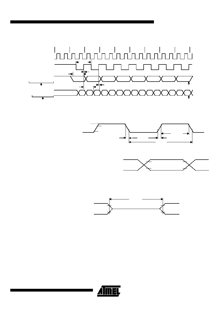
Shift Register Timing
Waveforms
External Clock Drive
Waveforms
AC Testing Input/Output
Waveforms
AC inputs during testing are driven at VCC - 0.5 for a logic “1” and 0.45V for a logic “0”.
Timing measurement are made at VIH min for a logic “1” and VIL max for a logic “0”.
Float Waveforms
For timing purposes as port pin is no longer floating when a 100 mV change from load
voltage occurs and begins to float when a 100 mV change from the loaded VOH/VOL level
occurs. IOL/IOH ≥ ± 20mA.
Clock Waveforms
Valid in normal clock mode. In X2 mode XTAL2 must be changed to XTAL2/2.
INPUT DATA
VALID
01
2345
6
8
7
ALE
CLOCK
OUTPUT DATA
WRITE to SBUF
CLEAR RI
T
XLXL
T
QVXH
T
XHQX
T
XHDV
T
XHDX
SET TI
SET RI
INSTRUCTION
01
2345
67
VALID
VCC-0.5V
0.45V
0.7V
CC
0.2VCC-0.1
T
CHCL
T
CLCX
T
CLCL
T
CLCH
T
CHCX
INPUT/OUTPUT
0.2 VCC + 0.9
0.2 VCC - 0.1
VCC -0.5V
0.45 V
FLOAT
VOH - 0.1 V
VOL + 0.1 V
V
LOAD
V
LOAD + 0.1 V
VLOAD - 0.1 V
发布紧急采购,3分钟左右您将得到回复。
相关PDF资料
PIC16C72A-04/SO
IC MCU OTP 2KX14 A/D PWM 28SOIC
AT89C51ID2-RLTIM
IC 8051 MCU FLASH 64K 44VQFP
AT89C51IC2-SLSIL
IC 8051 MCU FLASH 32K 44PLCC
AT89C51CC03U-RLTIM
IC 8051 MCU FLASH 64K 44VQFP
PIC24EP64MC204-I/PT
MCU 16BIT 64KB FLASH 44TQFP
AT89C51CC03U-RDTIM
IC 8051 MCU FLASH 64K 64VQFP
AT89C51CC03U-7CTIM
IC 8051 MCU FLASH 64K 64BGA
AT89C51CC03C-S3SIM
IC 8051 MCU FLASH 64K 52PLCC
相关代理商/技术参数
AT89C51RB2-3CSUL
功能描述:8位微控制器 -MCU 8-bit 16K Flash C51RB2 RoHS:否 制造商:Silicon Labs 核心:8051 处理器系列:C8051F39x 数据总线宽度:8 bit 最大时钟频率:50 MHz 程序存储器大小:16 KB 数据 RAM 大小:1 KB 片上 ADC:Yes 工作电源电压:1.8 V to 3.6 V 工作温度范围:- 40 C to + 105 C 封装 / 箱体:QFN-20 安装风格:SMD/SMT
AT89C51RB2-3CSUM
功能描述:8位微控制器 -MCU C51RB2 FLASH 5V 16k ind RoHS:否 制造商:Silicon Labs 核心:8051 处理器系列:C8051F39x 数据总线宽度:8 bit 最大时钟频率:50 MHz 程序存储器大小:16 KB 数据 RAM 大小:1 KB 片上 ADC:Yes 工作电源电压:1.8 V to 3.6 V 工作温度范围:- 40 C to + 105 C 封装 / 箱体:QFN-20 安装风格:SMD/SMT
AT89C51RB2L1-RLTUL
功能描述:8位微控制器 -MCU Microcontroller
RoHS:否 制造商:Silicon Labs 核心:8051 处理器系列:C8051F39x 数据总线宽度:8 bit 最大时钟频率:50 MHz 程序存储器大小:16 KB 数据 RAM 大小:1 KB 片上 ADC:Yes 工作电源电压:1.8 V to 3.6 V 工作温度范围:- 40 C to + 105 C 封装 / 箱体:QFN-20 安装风格:SMD/SMT
AT89C51RB2-RLRIL
功能描述:IC MCU FLASH 8051 16K 3V 44-VQFP RoHS:否 类别:集成电路 (IC) >> 嵌入式 - 微控制器, 系列:89C 标准包装:1,500 系列:AVR® ATtiny 核心处理器:AVR 芯体尺寸:8-位 速度:16MHz 连通性:I²C,LIN,SPI,UART/USART,USI 外围设备:欠压检测/复位,POR,PWM,温度传感器,WDT 输入/输出数:16 程序存储器容量:8KB(4K x 16) 程序存储器类型:闪存 EEPROM 大小:512 x 8 RAM 容量:512 x 8 电压 - 电源 (Vcc/Vdd):2.7 V ~ 5.5 V 数据转换器:A/D 11x10b 振荡器型:内部 工作温度:-40°C ~ 125°C 封装/外壳:20-SOIC(0.295",7.50mm 宽) 包装:带卷 (TR)
AT89C51RB2-RLRIM
功能描述:IC MCU FLASH 8051 16K 5V 44-VQFP RoHS:否 类别:集成电路 (IC) >> 嵌入式 - 微控制器, 系列:89C 产品培训模块:MCU Product Line Introduction
AVR® UC3 Introduction 标准包装:2,500 系列:AVR®32 UC3 B 核心处理器:AVR 芯体尺寸:32-位 速度:60MHz 连通性:I²C,IrDA,SPI,SSC,UART/USART,USB 外围设备:欠压检测/复位,DMA,POR,PWM,WDT 输入/输出数:28 程序存储器容量:128KB(128K x 8) 程序存储器类型:闪存 EEPROM 大小:- RAM 容量:32K x 8 电压 - 电源 (Vcc/Vdd):1.65 V ~ 1.95 V 数据转换器:A/D 6x10b 振荡器型:内部 工作温度:-40°C ~ 85°C 封装/外壳:48-TQFP 包装:带卷 (TR) 配用:ATSTK600-TQFP48-ND - STK600 SOCKET/ADAPTER 48-TQFPATAVRONEKIT-ND - KIT AVR/AVR32 DEBUGGER/PROGRMMRATEVK1101-ND - KIT DEV/EVAL FOR AVR32 AT32UC3B 其它名称:AT32UC3B1128-AUR-NDAT32UC3B1128-AURTR
AT89C51RB2-RLRUL
功能描述:8位微控制器 -MCU C51RB2 FLASH 3V 16k ind RoHS:否 制造商:Silicon Labs 核心:8051 处理器系列:C8051F39x 数据总线宽度:8 bit 最大时钟频率:50 MHz 程序存储器大小:16 KB 数据 RAM 大小:1 KB 片上 ADC:Yes 工作电源电压:1.8 V to 3.6 V 工作温度范围:- 40 C to + 105 C 封装 / 箱体:QFN-20 安装风格:SMD/SMT
AT89C51RB2-RLRUM
功能描述:8位微控制器 -MCU C51RB2 FLASH 5V 16k ind RoHS:否 制造商:Silicon Labs 核心:8051 处理器系列:C8051F39x 数据总线宽度:8 bit 最大时钟频率:50 MHz 程序存储器大小:16 KB 数据 RAM 大小:1 KB 片上 ADC:Yes 工作电源电压:1.8 V to 3.6 V 工作温度范围:- 40 C to + 105 C 封装 / 箱体:QFN-20 安装风格:SMD/SMT
AT89C51RB2-RLTCM
制造商:ATMEL 制造商全称:ATMEL Corporation 功能描述:8-bit Microcontroller with 16K/ 32K Bytes Flash